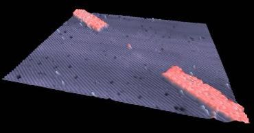
The tiny electronic device, described today in a paper published in the journal Nature Nanotechnology, uses as its active component an individual phosphorus atom patterned between atomic-scale electrodes and electrostatic control gates.
This unprecedented atomic accuracy may yield the elementary building block for a future quantum computer with unparalleled computational efficiency.
Until now, single-atom transistors have been realized only by chance, where researchers either have had to search through many devices or tune multi-atom devices to isolate one that works.
"But this device is perfect", says Professor Michelle Simmons, group leader and director of the ARC Centre for Quantum Computation and Communication at UNSW. "This is the first time anyone has shown control of a single atom in a substrate with this level of precise accuracy."
The microscopic device even has tiny visible markers etched onto its surface so researchers can connect metal contacts and apply a voltage, says research fellow and lead author Dr Martin Fuechsle from UNSW.
"Our group has proved that it is really possible to position one phosphorus atom in a silicon environment - exactly as we need it - with near-atomic precision, and at the same time register gates," he says.
The device is also remarkable, says Dr Fuechsle, because its electronic characteristics exactly match theoretical predictions undertaken with Professor Gerhard Klimeck's group at Purdue University in the US and Professor Hollenberg's group at the University of Melbourne, the joint authors on the paper.
The UNSW team used a scanning tunnelling microscope (STM) to see and manipulate atoms at the surface of the crystal inside an ultra-high vacuum chamber. Using a lithographic process, they patterned phosphorus atoms into functional devices on the crystal then covered them with a non-reactive layer of hydrogen.
Hydrogen atoms were removed selectively in precisely defined regions with the super-fine metal tip of the STM. A controlled chemical reaction then incorporated phosphorus atoms into the silicon surface.
Finally, the structure was encapsulated with a silicon layer and the device contacted electrically using an intricate system of alignment markers on the silicon chip to align metallic connects. The electronic properties of the device were in excellent agreement with theoretical predictions for a single phosphorus atom transistor.
It is predicted that transistors will reach the single-atom level by about 2020 to keep pace with Moore's Law, which describes an ongoing trend in computer hardware that sees the number of chip components double every 18 months.
This major advance has developed the technology to make this possible well ahead of schedule and gives valuable insights to manufacturers into how devices will behave once they reach the atomic limit, says Professor Simmons.


Reader Comments
to our Newsletter