At the semiconductor industry conference Semicon in Tokyo today, IBM photonics leader Yurii Vlasov is detailing how IBM has created a chip that integrates many of the necessary elements of optical communication between a processor and other devices. Significantly, the design uses conventional rather than exotic chip manufacturing technology, involves very small components, and essentially permits a fiber-optic communication line to be attached directly to a processor.
And more significantly, it's headed for real-world use, a sign that IBM's work is serious. That initial use is in IBM's relatively exotic Exascale project to build a computer that can perform a quintillion mathematical calculations per second--roughly 1,000 times that of today's fastest supercomputers.
"In three to five years, silicon photonics will be the main enabler for that level of computation," said Solomon Assefa, an IBM research scientist and one of the members of the team that developed the chip. And in the years after that, it'll follow the traditional computing industry trend and spread to more ordinary products, he predicted.
IBM's project is called SNIPER--short for "silicon nanoscale integrated photonic and electronic transceiver"--but the company is labeling it with the slightly less ungainly term of silicon nanophotonics. It's been under way for a decade, an indicator of just how difficult it is to develop.
The technology is a breakthrough and shows Big Blue well ahead of competitors such as Intel and Samsung, said Envisioneering Group research director Richard F. Doherty. Much previous work about optical connections involved much larger devices that were separate from the processor itself, he said.
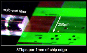
This image shows how an optical fiber can be connected directly to the chip.
Specifically, IBM said a transceiver that can send and receive signals measures 0.5 square millimeter, and a single-chip transceiver with a capacity of 1 terabit per second could fit on to a chip measuring 16 square millimeters.
"We expect Intel and Samsung will dust off some optical research and home in on what IBM has now proven," Doherty said.
Assefa is keenly aware of where his competitors stand. "We're many steps ahead of Intel," he said, but one start-up, Luxtera, has silicon photonics products now on the market. In November, it announced silicon photonics links that can transfer data at 25 gigabits per second.
Optical communications, which today are used chiefly for heavy-duty networking tasks such as the core of the Internet, have advantages over the more conventional method of sending electrical signals over wires. For one thing, optical communications use less energy and can span longer distances. For another, sending light down optical fibers enables tremendous data transfer capacity--in part because a technology called wave division multiplexing means that multiple colors of light can be sent simultaneously to pack even more capacity into each communication link.
But optical communication technology is expensive. It's expanding to premium services such as Verizon's Fios and BT's Infinity and to Intel's Light Peak high-end computer connection technology, but costs are still high. What IBM's Sniper project does is bring down the cost by marrying it to the semiconductor chip manufacturing industry.
IBM's technology today consists of a processor with six optical communication links. The chip itself has six transmitters and receivers, each capable of handling eight channels of data through the multiplexing technology. Also built in are modulators, which control the laser that generates the light signals--though the laser itself is a separate component. Each modulator can manage bandwidth of 20 gigabits per second, a major step toward IBM's goal of a chip with an aggregate capacity 50 times that, 1 terabit per second.
For reference, today's conventional Ethernet operates at 1Gbps per second and sometimes at 10Gbps in higher-end servers. A capacity of 1Tbps would be enough to transfer the data of 26 DVDs in a second.
Building links into silicon makes them cheaper to manufacture and therefore more mainstream. "A single high-performance computing machine will contain a similar number of optical communication channels as currently exist in all parallel optical links worldwide," Vlasov said in his presentation.
The photonics work initially will be used over relatively long distances, connecting separate computers or groups of computers housed in racks. Ultimately, though, IBM expects it to be used within a processor, connecting the independent processing cores, Assefa said.
While IBM has been a pioneer in processor manufacturing and hasn't yielded to more powerful chipmakers such as Intel, its fabrication volume tends to be low by industry standards. It uses those chips in premium products, though, such as its own servers and mainframes, and its research gives it clout when it comes to patent licensing partnerships with rivals. IBM has more than 30 base patents involved with silicon photonics, the company said.
One problem with sending lots of data over electrical wires is that it requires significant electrical power--and much of that is lost to waste heat that holds back processing speeds and requires extensive engineering within computers and data centers to keep things cool. Light-based communication reduces that problem.
"A large part of computer power draw is the high-speed buses and cabling between cards and modules and systems. If even a small number of system go optical, processing efficiency and power savings will both soar," Doherty said.
In addition, high-speed electrical communication produces electromagnetic waves that interfere with neighboring electrical operations, since each tiny wire in a computer can act as an antenna. With optical communications, that interference is reduced, Doherty said, with one benefit being that it's easier to develop low-power chips because there's less need to overpower all the interference.
The next steps for IBM are to focus on efficient, reliable manufacturing of its silicon photonics products and building it into its exascale supercomputer. After that, eventually, it will be a part of a larger industry spreading the light farther.
"The way technology works, usually those [supercomputer] technologies find their way in five to ten years back into the lives of ordinary people," he said. "Down the road i'm sure the tech will find its way into the lives of all of us."


Reader Comments
to our Newsletter